Principle:
Scanning electron microscopy (SEM) is an electron microscopy technique that can analyse a visual image of a sample with high-quality and spatial resolution using an electron beam in nanometer scale. It gives information about topography, morphology, composition, and other properties of a sample. In SEM, two types of electrons are detected: backscattered electrons (BSE) and secondary electrons (SE). Backscattered electrons are reflected back after elastic interactions between the beam and sample while secondary electrons originate from the atoms of the sample. Hence, SE are a result of inelastic interactions between the electron beam and the sample.
Current Model

Hitachi SU-70 Field Emission Gun Scanning Electron Microscope
See video for further information
Scanning Electron Microscope
The main SEM components include source of electrons, column down which electrons travel with electromagnetic lenses, electron detector, sample chamber, and computer and display to view the images.
The Hitachi SU-70 is a high-resolution field emission scanning electron microscope capable of high-resolution imaging (1.0 nm at 15KV). It features several specialised in-lens detectors in addition to STEM (Scanning TEM) and Oxford Instrument EDX/WDX (Energy Dispersive X-ray analysis and Wavelength Dispersive X-ray analysis) capability. Furthermore, it allows reduced charge-up imaging and low voltage imaging.
Typical samples:
Samples which are analysed may include metals, polymers, coated components, powders etc. The SEM utilizes vacuum conditions and uses electrons to form an image; therefore, special preparations must be made with the sample:
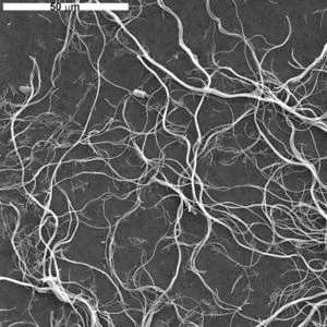
Representative SEM image of Asbestos
Typical Preparation Steps:
- Wet Samples:All water must be removed from the samples because the water would vaporise in the vacuum.
- Metal Samples:All metals are conductive and require no preparation before being used.
- Non-Metal Samples:All non-metals need to be made conductive by covering the sample with a thin layer of conductive material. This is done by using a device called a “sputter coater.”
- The SEM is critical in all fields that require characterisation of solid materials. Most SEMs are comparatively easy to operate, with user-friendly “intuitive” interfaces. Many applications require minimal sample preparation. However, the SEM Samples must be solid, and they must fit into the microscope chamber. Maximum size in horizontal dimensions is usually on the order of 10 cm; Vertical dimensions are generally much more limited and rarely exceed 40 mm. For most instruments’ samples must be stable in a vacuum on the order of 10-5 – 10-6 torr.
Technical Specifications:
- Schottky (thermal) field emission electron source
- Imaging resolution of 1nm at 15 KV and 1.6nm at 1 kV
- Magnification: Low mag. mode 20x – 2000x; High mag. mode 100x – 800,000x
- Accelerating Voltage: 0.5 kV – 30 kV
- Probe Current: 1 Ρa to >200 Na.
- Specimen Stage: x = 110 mm, y = 110 mm, z = 1.5 – 40 mm, tilt =-5 – +70 degrees
- Flexible Detection System utilising: Highly efficient in lens, Lower and Upper
- Secondary Electron Detectors, Low and High Angle Backscattered Electron Detectors and STEM Detector.
- Anti-Contamination Trap “Cold Finger” used to reduce sample contamination.
Standards:
Samples can be accessed in accordance with the other standards such as: ASTM E986 – 04(2017), ASTM E2809 – 13, ASTM C1723 – 16, ASTM F1372 – 93(2020), ASTM E2142 – 08(2015), ASTM E766 – 14(2019), ISO 21466:2019, ISO 22493:2014